


Our transform imager technology [3, 1] and architecture allows for retina and higher-level bio-inspired computation in a programmable architecture that still possesses similar high- fill factor pixels of CMOS imagers. The high-fill factor means that we can achieve these additional signal processing computations in roughly the same area and effectively at lower power consumption as typical current CMOS imagers. This approach enables programmable image signal processing in very low-power architecture; one could envision an imager plus the computation of a block 2D matrix transform, like 2D DCT transform in a megapixel imager consuming between 100 microWatts and 1mV.
In current megapixel imagers, one consumes over a Watt of power for the imager and Analog-to-Digital Converter. In a similar structure and resulting chip area, we can have a single chip image JPEG compression or single chip image enhansement computation consuming less power than a typical imager and analog-to-digital converter. One can easily compute additional transforms with minimal computational complexity, such as optical flow or depth from stereo computations. These approaches will be essential in low-power portable applications, such as hand-held teleconferencing, low-power tracking devices, and preprocessing for retinal prosthetics. We see this imager technology as an excellent candidate for Cooperative Analog-Digital Signal Processing (CADSP) approaches towards image and other two-dimensional signal processing [5]. We discuss elsewhere the comparison of this imager to CMOS imagers and Focal-Plane imagers [1, 2].
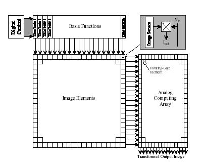 |
Figure 1: Top view of our matrix transform imager. Our approach allows arbitrary separable matrix image transforms directly on the CMOS imager pixel data prior to A/D conversion; these transforms are programmable because we use floating-gate circuits. Each pixel processor multiplies the imconing input with the measured image sensor result, and outputs a current of this result. |
Figure 1 shows the block diagram of our transform imagers. If the incoming voltages represent functions in time, particularly transform bases like sine and cosine, then we are performing computations analogous to matrix image transforms. The output is a continuous stream of each row of the transformed image, repeated over a desired fundamental frequency. This approach is enabled by floating-gate circuits [4], in storing arbitrary analog waveforms for image transforms,in programming waveforms to account for average device mismatch, and in computing additional matrix-vector computations.
This imager is capable of programmable matrix operations on the image, where we can represent the image as either a full matrix or using block matrix operations. The core imager performs computation at the pixel plane, but still holds to a fill factor greater than 40 percent. Each pixel is composed of a photodiode sensor element and an analog multiplier [2] and could be directly read out by this technique, since a column scan is equivalent to multiplication by a digital value moving by one position for each step. From our measurements in standard room light levels, we expect sufficient sensor bandwidth for a 1024 x 1024 imager performing full matrix operations at 60Hz image rate.
This Transform imager can compute arbitrary separable matrix transforms. We perform separable matrix transforms as Y = (A^T)PB where P is the row and column array of pixels, Y is the computed output image array, A is a transform matrix corresponding to the transform on the image plane by the basis functions, and B is a transform matrix corresponding to the floating-gate enabled transform after the image plane. The values of A are stored in an analog floating-gate array typically on the imager IC, and applied to the pixel column inputs. Further, if the input waveforms are continuous, then the result is a continuous waveform, resulting in added computational options. For example, the choice of output signal sampling will result in di erent discrete-time inspired computations with an identical setup. For this paper we will concentrate on computing a DST / DCT like transforms of the image as a representitive of possible matrix computations. To characterize this imager, we will compute these transforms for uniform illumination; the ideal DST would be all zeros, and the ideal DCT would be an impulse at position (1,1).
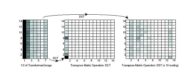 |
Figure 2: Experimental data from a 14 x 14 test imager. We present one half of the output image after transforming the image (uniform illumination) using sine waves. The output image is symmetric; therefore we have output only the first half. Sampled at integer points. DCT Transform: Result of an additional Cosine transform on initial sine-transformed imager data. We nearly get the ideal impulse function at (0,0) position, as predicted by taking a 2D Cosine transform of an image of uniform illumination. DST Transform: Result of an additional Sine transform on initial sine-transformed imager data. The plot of this Sine transform multiplied by a factor of 10 in comparison with the Cosine transform; without the scaling factor (x 10), the image would look nearly white. We get nearly zero matrix as we would expect for an input image of uniform illumination.
Figure 2 shows the experimental results of DST/DCT type transforms on a uniformly illuminated image from a small 14*14 image block, requiring roughly 150*200micrometer for the array in 0.5micrometer. We input sine waves of integer frequencies and obtained the rst image result by sampling at TT/2 phase of the primary harmonic (This transform is symmetric, so we show only the first half of the output waveform). From the resulting waveforms (not sampled waveforms), we computed the second matrix transform using DST coeffcients and then for DCT coeffcients. We see some distortion in the transformed images, which correlates well to harmonic distortion from the differential pairs. Since the input patterns are fixed, the effect of harmonic distortion is fixed and appears as additional spatial (smoothing) lter. In practice we can account for this additional linear spatial filter, by modifying the matrix transform coeffcients to account for this filter. In the same process, we have built a functional 128*128 imager with matrix processing for 16 x 16 block transforms in an area of 4 millimeter square in the same process, and have fabricated a 512*512 imager in a 0.25 micrometer process with matrix processing for 64 x 64 block transforms in an area of 8 millimeter square.
References
[1] Paul Hasler and Abhishek Bandyopadhyay. A matrix transform imager and architecture. In IEEE Sensors, Orlando, June 2002.
[2] Paul Hasler, Abhishek Bandyopadhyay, and Paul Smith. A matrix transform imager allowing high fill factor. In Proceedings of the IEEE International Symposium on Circuits and Systems,Phoenix, AZ, May 2002.
[3] Paul Hasler, Abhishek Bandyopadhyay, and David V. Anderson. Low-power analog image processing using transform imagers. In IEEE Midwest Circuits and Systems, Tulsa, OK,August 2002.
[4] Matt Kucic, Paul Hasler, Je Dugger, and David V. Anderson. Programmable and adaptive analog lters using arrays of floating-gate circuits. In Erik Brunvand and Chris Myers, editors,2001 Conference on Advanced Research in VLSI, pages 148-162. IEEE Computer Society,March 2001.
[5] P. Hasler and L.A. Akers. A continuous-time synapse employing a multilevel dynamic memory. In Proceedings of the International Joint Conference on Neural Networks, volume 1, pages 563-568, Seattle, WA, 1991.
back to Key Technologies