
Power and Resolution in Analog Signal Processing
As embedded computing becomes mainstream, a significant market has emergedfor feature-rich signal processing devices that consume very little power.
While digital processors can perform the desired functions, there are many cases where an analog design could offer the same functionality at a fraction of the power required for the digital solution.
For example, the analog multiplier presented later in this paper requires only two floating-gate transistors and two small DIBL transistors operating in the subthreshold region. Kucic, et. al.
[10]
show that this kind of multiplier can easily provide 10 bits of resolution. Now, consider a digital 10-bit multiplier requiring thousands of transistors.
In this case, the power savings of the analog version are at least three orders of magnitude over the digital implementation.
Another primary concern in signal processing is the resolution. Sarpeskar [11] showed that an analog computation can have significant advantages over a digital solution when the resolution of the inputs is around 10 bits or less. Experiments with the floating-gate devices done at the Goergia Institute of Technology have confirmed that analog implementations work well within this resolution range.
Floating-gate Transistors
The floating-gate transistors used in these FPAAs are standard pFET devices whose gate terminals are not connected to signals except through capacitors
(e.g., no DC path to a fixed potential)
[12].
Because the gate terminal is well insulated from external signals, it can maintain a permanent charge, and thus, it is an analog memory cell similar to an EEPROM cell. With a floating gate,
the current through the pFET channel is dependent on the charge of the floating-gate node.
By using hot-electron injection to decrease the charge on the floating-gate node and electron tunneling to increase the charge on the floating-gate node,
the current flow through the pFET channel can be accurately controlled
[12][10].
Floating-gate Switches
Using a floating-gate transistor as a switch requires that the device be turned "on" or turn "off." Ideally,
the "on" state corresponds to the free flow of current through the device or equivalently, zero impedance between the source and the drain.
Likewise, the "off" state is characterized by zero current flowing through the device- an infinite impendance between the source and the drain nodes.
A floating-gate transistor, however, will not act as a perfect switch. The "on" state will be characterized by an impedance greater than zero,
and the "off" state will have an impedance less than in?nity. Therefore, the quality of a floating- gate transistor as a switch will be determined by measuring the "on" and "off" impedances.
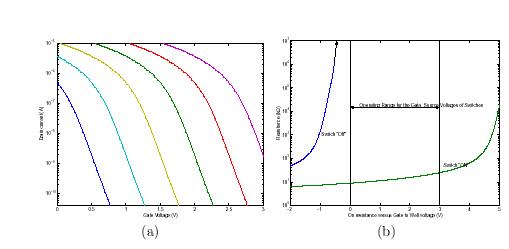 |
Figure 1: (a) This is a current-voltage plot of a single floating-gate transistor programmed to different levels of floating-gate charge. The floating-gate transistors can be programmed over a wide range of currents. (b) This plot shows the resistance versus gate voltage for a single floating-gate transistor programed to the "on" level and to the "off" level. |
The quality of the switches is an important factor in determining the final architecture. The main concern is that routing a signal through multiple switches could degragate data as the cummulative impedance of the switches becomes prohibitive.
The impedance of the floating-gate transistor is a function of the charge on the fioating-gate node allowing it to be set using hot-electron injection and electron tunneling. Figure 1(a) shows the relative I-V curves for a floating-gate transistor as it is programmed from "off" to "on." Ideally, each transistor would be programmed to the extreme ends of the graph, but programming floating- gate transistors is a time-comsuming task. The desired quality of the switch will have to be choosen with regard to the time it will take to program the device.
Choosing a reasonable time scale for programming leads to a compromise in the quality of the switch. Also, note that the operating voltage of the gate node is not fixed. Due to the parasitic capacitances between the gate and drain/source nodes, the gate voltage- and thus the switch's impedance-will vary as a function of the signal current. This variation must be minimized. The final selection of "on" and "off" impedances is shown in Figure 1(b). This choice takes into account the trade-offs between programming time and switch quality.
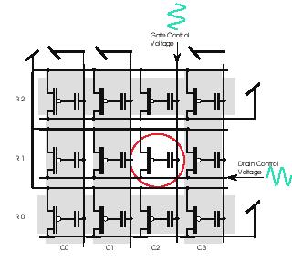 |
Figure 2: By selectively setting the gate and drain voltages of the columns and rows, a single floating-gate transistor can be programmed using hot-electron injection without affecting the neighboring devices. |
Switch as Computational Element
When used as a switch, the floating-gate should be as transparent a part of the circuit as possible.
However, Figure 1 shows that the floating-gate transistor can be used as an in-circuit element
[13][14].
By adjusting the charge on the floating-gate node between the extremes used for "on" and "off",
the impedance of the switch can be varied over several orders of magnitude.
Using the floating-gate switches as in-circuit elements allows for a very compact architecture.
The physical area needed for the CABs is reduced greatly,because resistors,
which consume relatively large amounts of space on CMOS processes, are not needed as separate components.
By reducing the number of individual circuit elements, signal routing is simplified, while not loosing functionality.
Programmability
By using floating-gate devices as the only programmable element on the chip,configuring the chip is greatly simplified.
Additionally, all of the floating-gate transistors are clustered together to aid in the programming logic and signal routing.
Decoders on the periphery of the circuit are connected to the drain,source, and gate (through a capacitor)
terminals of the floating-gate matrix.During programming mode, these decoders allow each floating-gate transistor to be individually programmed using hot-electron injection (see Figure 2)
[10].
Part of our previous effort was to develop a systematic method for programming arrays of floating-gate transistors [10][13][15]. A microprocessor-based board has been built to interface a PC to these analog floating-gate arrays for the purposes of programming and testing. With a PC controlling the programming of these devices, the details of using hot-electron injection and tunneling to program individual floating-gate switches have been abstracted away from the end-user. The programming algorithms have been optimized for accuracy and speed, while giving the end-user an easy-to-use interface for configuring arrays of floating-gate devices.
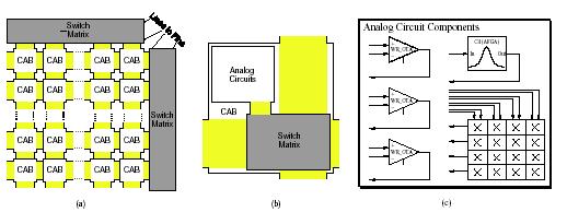 |
Figure 3: Block diagram of our generic FPAA chip. (a) Architecture diagram of analog programmable computing blocks. Future FPAAs will have 100 or more ComputationalAnalog Blocks (CAB) each with 23 ports to the mesh switching matrix. (b) Signal flow in a single CAB. (c) Each Computational Analog Block (CAB) has a four-by-four matrix
multiplier, three wide-range operational transconductance amplifiers
(OTAs),and a capcatively coupled current conveyor (C4). The input
and output signals shown in this figure are routed to the rows of
the switch matrix. |
FPAA Architecture
Large signal processing systems will require a chip with many (100 or more) computational analog blocks (CABs) on it.
However, before such a chip can be successfully designed, a number of implementation details need to be tested on a smaller scale.
Specifically, the switching characteristics of floating-gate transistors have not been studied in detail before.
We have developed RASP (Reconfigurable Analog Signal Processor) as a testbed integrated circuit (IC) to study the floating-gate switches,
and the interaction between the CAB components and the switch matrix.
It was determined that two CABs would be adequate for a first run. Once favorable results are shown on RASP,
a larger chip will be abricated by replicating the basic blocks found on this chip.
CABs
The computational logic is organized into a compact computational analog block (CAB) providing a naturally scalable architecture.
CABs can be tiled across the chip with busses and local interconnects in-between as shown in Figure 3.
Each CAB is comprised of components critical to signal processing applications including a four-by-four matrix-vector multiplier,
three wide-range operational transconductance amplifiers (OTAs), and a transistor-only version of the autozeroing floating-gate amplifler (AFGA)
or capacitively coupled current conveyor (C4)
[16].
The CAB architecture is shown in Figure 3(c).
Analog Circuit Components
Selecting the types of analog components to include in a general-purpose FPAA is a diffcult task. To be as universal as possible,
one must consider adding a number of basic linear and nonlinear functions including integration, summation, gain amplification,
logarithmic and exponential operations, and more
[17].
Because these elements are so basic, constructing larger systems can become very complex because of the routing resources required.
Also, as discussed earlier, as the number of switches involved in a circuit increases the cummulative effects of the switches on the circuit may seriously degrade the performance and/or results.
To mitigate these challenges, RASP was constrained to be a signal-processing FPAA with specific functions such as adaptive filtering and Fourier (frequency domain) processing in mind.
A limited number of basic elements were also included for completeness;
however, the focus was placed on selecting an appropriate mix of higher-level components that could facilitate the prototyping of a wide range of problems.
Basic Analog Elements
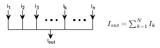
The basic analog functions such as summation, integration, and gain amplification can be included in the FPAA with only a few analog components.
In the case of summation, only the switch matrix is needed.Figure 4a shows that if the input signals are currents,
summation is achieved by simply connecting the input signals together (Kirchoff's current law).
 |
By adding several configurable operational transductance amplifiers (OTAs) to each CAB, one can configure the FPAA to perform integration, differentiation,gain amplification and more. Also, by including op-amps in the computational logic, RASP can compete with current commercial offerings that are based solely on programmable op-amps.
 |
Matrix-Vector Multiplication
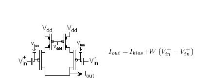
Multiplication is an important element in many signal processing applications.
Figure 5 shows a basic multiplier using two floating-gate transistors.
The differential voltage input allows signed numbers to be represented.
The multiplier's functionality can be extended by cascading them together to form a matrix-vector multiplier.
Each CAB on RASP has a four-by-four matrix multiplier in which four signed (differential) inputs are mutliplied by a four-by-four matrix of programmable weights.
Of course, by setting the appropriate weights to zero a single multipy, or a four-by-one, four-by-two,or four-by-three matrix-vector multiply can also be accomplished.
Filtering and Fourier Processing
In the near future, FPAA devices based the Matix II's floating-gate architecture will have as many as 100 or more CABs on a single chip.
At this level of complexity a number of interesting signal processing systems can be implemented using a Fourier processor.
An analog Fourier processor decomposes an incoming signal into its frequency components (sub-bands).
Each sub{band is then operated on before reconstructing the output signal by summing the sub-bands together.
This is analagous to digitally taking an FFT, operating on each frequency component, and then taking an IFT to generate the time-domain output signal.
In RASP, the frequency decomposition is done by using capacitively coupled current conveyor (C4) circuits to band-pass filter the incoming signal.
A C4 circuit is built using two floating-gate transistors and several capacitors as shown in
[18][10].
This method allows the band-pass fllters to be programmbly placed at the desired frequencies
(e.g., some applications prefer linear spacing while others prefer logarithmic spacing of the sub-bands).
When used in combination with the floating-gate multiplier, a wide range of fllters, including adaptive filters, can be achieved
[12].
Switch Matrix
RASP has one 16 by 64 switching matrix that provides local interconnects between the two CABs and connections to the external input/output signal lines.
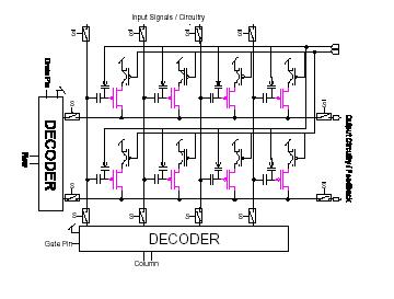 |
Figure 6: The switching matrix is built with floating-gate transistors. The charge of the floating-gate node can be adjusted to allow current to flow through the channel ("on") or to restrict current flow ("off"). When in programming mode, T gates connect the floating-gate transistors to the decoders, and when in operational mode,the decoders are unconnected and the output signals are switched on. |
The switching matrix uses floating-gate transistors as the switches as shown in Figure 6. The digital decoders on the outside of the the switch matrix provide access to the individual floating-gate transistors for programming. After programming is complete the decoders are disconnected (using t-gate switches) and external bus lines are connected to start the operation of the chip.
The source lines of the 16 floating-gate switches in each row are connected together; likewise, the drain lines of the 64 floating-gate switches in each column are tied together. Programming a switch to "on" allows current to flow in the source-drain channel and connects a row with a column. Programming a switch to "off" restricts the current flow in the channel creating a very high impedance betweenthe row and column.
The input/output signals from each CAB are connected to the sources nodes of the floating-gate switches. The drain nodes (columns) are either connected to external busses or are used for internal connections only. By doing this, any input/output signal from the CABs can be connected to an external bus by turning on one floating-gate switch. Similarly, it can be connected to another signal in the same CAB or to a signal in an adacent CAB by turning on two switches in the same column.
Digital Control and Interface
Today, signal processing is a largely digital domain. Similarly, even if a given algorithm can be implemented in analog alone,
the results will more than likely need to be accessed by a digital processor.
To make this technology more flexible and more useful to signal processing engineers, this FPAA has a completely digital interface.
From programming to operation, all communication to and from these FPAAs is digital.
On-chip analog-commercial and academic settingsto-digital (A/D) and digital-to-analog (D/A) converters provide the domain conversions for input and output signals.
Likewise, programming operations are turned on and offusing digital control logic.
System Integration
With a digital interface, FPAAs can be easily connected to FPGAs, PCs, and embedded devices such as handheld computers and cell phones.
In this way,rapid prototyping of mixed-mode systems can easily be accomplished. A mixed-mode prototyping station is the natural outcome of this technology.
A single board with both an FPAA and an FPGA mounted on it will be a significant advancement for the rapid prototyping of mixed-mode systems.
Programming
The programming of FPAAs is achieved through a digital interface.
Digital switches control the tunneling and injection voltages and the digital decoders provide individual access to the floating-gate transistors.
An on-chip, specialized A/D converter provides feedback to the programmer by outputting a digital signal with a pulse width
that is proportional to the drain current of the floating-gate transistor currently being programmed.
To avoid additional hardware on the prototyping station,
the FPGA that is used to implement the digital part of the system in operational mode is used to implement the programming algorithms in configuration mode.
